Technical Support
 Feedback



One of the trends in the development of the microelectronics industry is the gradual miniaturization of devices, i.e., the increasing integration density of transistors on a chip. This brings higher power density and heat generation, which in turn places higher demands on heat dissipation. The heat dissipation problem has also become a core bottleneck constraining chip miniaturization. On the other hand, the energy consumption required for cooling electronic components is increasing day by day, and the resulting environmental issues cannot be ignored (1).
Microchip Design with Integrated Cooling System
In conventional device design, device circuits and cooling systems are often designed independently, resulting in low cooling efficiency and difficulty in properly addressing energy consumption issues. Recently, a research team at EPFL (École Polytechnique Fédérale de Lausanne) proposed the concept of integrating circuit modules and cooling modules on a chip, demonstrating excellent heat dissipation performance. The related research results were published in Nature (2). The team designed the microfluidic channels required for the cooling system very close to the heat-generating transistors. The coolant flows through channels at the bottom of the chip into the microfluidic channels, efficiently cooling the transistors and preventing heat from spreading across the entire chip and degrading performance (see the animation in Figure 1).

Figure 1 Animation demonstrating heat dissipation by coolant flowing through microchannels on the backside of the chip (cross-sectional view).
This research is of significant importance for improving device cooling efficiency and reducing energy consumption, and is expected to increase transistor integration density and further extend the limits of Moore's Law. The authors designed a monolithically integrated manifold microchannel (mMMC) cooling system, placing the microfluidic channels beneath the electronic devices. The cross-sectional view is shown in Figure 2a: the electronic device layer is located on the GaN epitaxial layer, beneath which are the microchannels through which the coolant flows. The coolant channels and device patterns are sealed by a copper layer (Figure 2b), and the bottom of the chip contains larger-width main heat dissipation channels fabricated by backside etching (Figure 2c). The core design innovation of this chip lies in the integration of microfluidic channels, and the specific implementation scheme is as follows (Figure 2d):
Prepare an AlGaN/GaN epitaxial layer on a silicon wafer;
Fabricate micron-scale slits on the epitaxial GaN layer and perform anisotropic deep etching (depth 100 μm);
Use XeF2 gas isotropic etching technology to fabricate wide channels in the silicon layer;
Then seal the micropores on the GaN layer by electroplating copper.
Finally, electronic devices are fabricated directly above the channel array cooling system. This co-design approach enables uniform and efficient cooling at low pumping power. The embedded design uses a low-cost silicon layer to fabricate coolant channels, saving the cost of high-thermal-conductivity substrates compared with conventional chip designs.
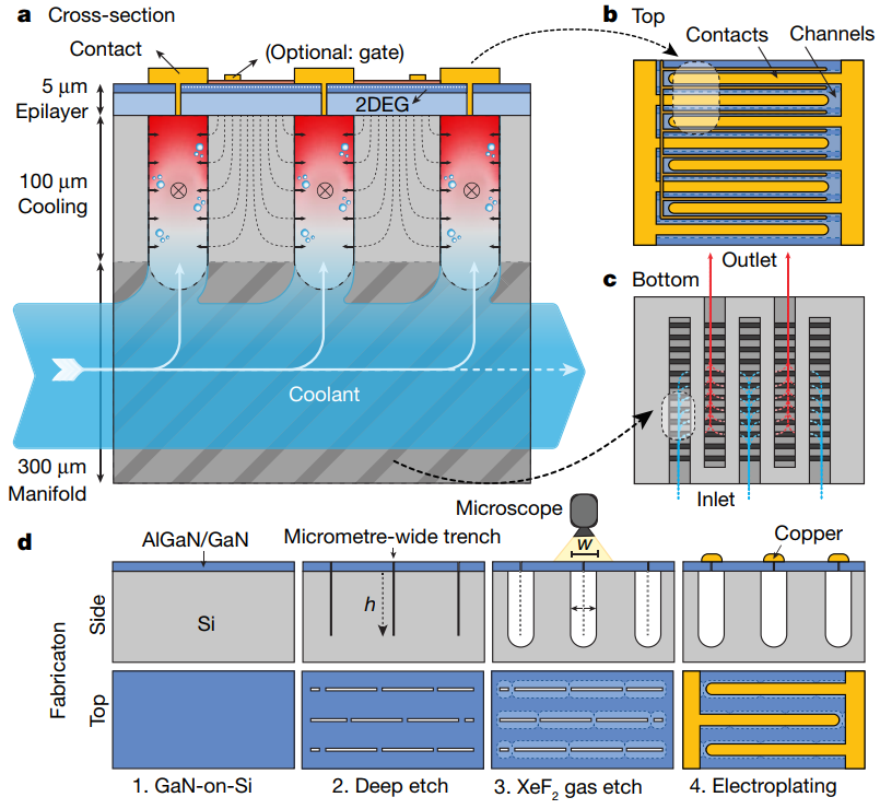
Figure 2 Schematic of an electronic chip with an integrated microfluidic cooling system.
a. Schematic of the device structure; b. Top view of the chip; c. Side view of the chip; d. Schematic of the chip fabrication process flow.
Cooling Performance Evaluation
In this work, the authors compared the heat dissipation efficiency of straight, parallel microchannels (SPMCs) and the mMMC scheme using different cooling structures. The microstructural images of SPMC and mMMC are shown in Figures 3a and 3b, respectively. For the SPMC scheme, the heat dissipation efficiency gradually improves as the channel width decreases, but the required pumping pressure increases accordingly. To achieve a flow rate of 0.5 mL/s, SPMCs with widths of 100 µm, 50 µm, and 25 µm require pressures of 160 mbar, 260 mbar, and 810 mbar, respectively, which means the energy consumption for heat dissipation increases significantly. The mMMC design can significantly reduce the pressure drop by shortening the flow path length of the microchannels. When a 10-channel manifold is used to split the flow into smaller portions, the pressure required is only 210 mbar, meaning that the mMMC design can achieve high heat dissipation efficiency at lower pumping power.
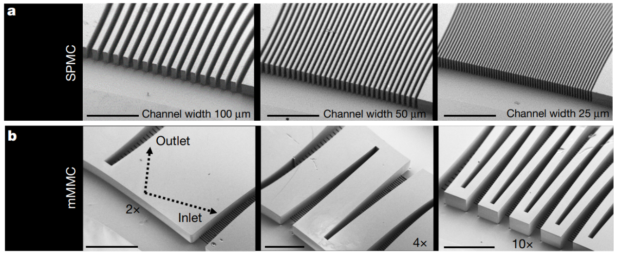
Figure 3 Structural diagrams of microchannel cooling systems.
a. Electron microscopy characterization of the straight, parallel microchannel (SPMC) structure, scale bar width 1 mm; b. Electron microscopy characterization of the monolithically integrated manifold microchannel (mMMC) structure, scale bar width 0.85 mm.
Using deionized water as the coolant, a heat flux as high as 1723 W/cm2 can be achieved on the 10-channel manifold mMMC structure. Compared with their previous scheme (25 μm-wide SPMCs), the cooling coefficient of performance (COP) of the 10-channel manifold mMMC structure is improved by a factor of 50. The authors further compared the heat flux and COP values of various coolers reported in the literature, and it can be seen that this mMMC design has superior cooling performance (Figure 4).
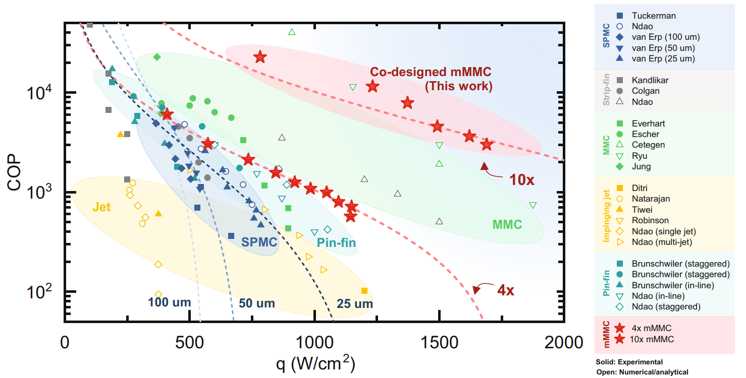
Figure 4 Coefficient of performance (COP) of various coolers.
Example of a Power Integrated Circuit with Embedded Cooling
The authors used the embedded scheme to fabricate an AC-DC converter, with channels designed on a printed circuit board to allow coolant to enter and exit. They monolithically integrated a full-bridge rectifier onto a single GaN-on-Si chip, using four Schottky barrier diodes to achieve the rectification function, with 50 µm-wide cooling channels integrated in the silicon substrate (Figure 5a). By designing a printed circuit board (PCB) with a coolant flow system, the coolant can be introduced to the backside of the chip (Figure 5b). Physical photographs of the AC-DC converter with the integrated microchannel cooling system are shown in Figures 5c–d, demonstrating the high compactness of this design. As shown in Figure 5e, the device array can rectify AC signals with peak voltage and current of 150 V and 1.2 A. Compared with air cooling, the liquid cooling scheme has significantly higher conversion efficiency (Figure 5f), and at an output power of 120 W, the temperature change can be maintained below 50 K (Figure 5g). Based on the device area, the power density is calculated to be as high as 25 kW/dm3. This means that the cooling scheme is expected to enable applications of high-power devices (exceeding kilowatts) in the future.
TEL: 0731-85260926 Fax: 0731-85263946 E-mail: sales@jectronic.com Address: Room 1015, Building A3, Changsha Yu Center, No. 289 Huanbao Middle Road, Yuhua District, Changsha City Copyright © Changsha Ligao Jiechuang Instruments Co., Ltd. Copyright Jectronic instruments ltd, All Rights Reserved For more information, please follow our WeCom.