 Technical Support
 Feedback


Why Test Chips?
Compiled by: Changsha Ligao Jiechuang Instrument Co., Ltd.
Chip testing is a broad topic that runs throughout the entire chip design and production process.
First, a chip can fail in the following ways:
Functional failure: a particular function is not implemented. This is usually a design issue, and is normally prevented by pre-silicon simulation to verify functionality during the design phase. That is why simulation and verification typically consume about 80% of the time when designing a chip.
Performance failure: a performance spec is not met. For example, a 2G CPU only reaches 1.5G; an ADC that must achieve 12-bit ENOB at the required conversion rate and bandwidth only reaches 10 bits; or an LNA misses its noise figure target. This usually stems from two causes: insufficient margin in the initial system design, or a poor physical layout. Such issues are typically verified through post-layout simulation.
Production-induced failure. The cause lies in monocrystalline silicon production. Anyone who has studied semiconductor physics knows that monocrystalline silicon has a regular face-centered cubic structure with several crystal orientations; single crystals are typically grown by the Czochralski process along the <111> direction. However, external factors such as temperature, pull rate, and various quantum-mechanical random effects can introduce dislocations during growth, which are known as defects.
Another source of defects is ion implantation, which can leave irregular structures that annealing fails to correct. These problems in the semiconductor cause device failure and, in turn, affect the entire chip. To screen out failed or partially failed chips after production, dedicated test circuits are added at design time—such as test muxes in analog blocks, scan chains (logic test), MBIST (memory test), and boundary scan (IO and bonding test) in digital blocks—to ensure that only good chips are delivered to customers. Failed or partially failed products are either scrapped or downgraded and sold as lower-tier products.
Detecting these chip failures requires chip testing.
At What Stage Is Chip Testing Performed?
Chips are now larger than ever, making testing quite challenging. How to test is therefore a deep discipline. With so many signals, it is impossible to bring every signal out for testing, so design-for-testability (DFT) must be built in at design time.
DFT, in short, means observing internal signals indirectly through methods such as scan chains, then testing with specialized test equipment. This is not a simple oscilloscope—it must generate various test waveforms and detect the outputs, so a complete platform costs around a million yuan. DFT is better suited to small chips; large chips such as CPUs also use built-in self-test (BIST), which lets the chip run tests itself at power-up and greatly reduces the test engineer's workload.
Once DFT testing passes, the formal chip test stage begins.
By test object, testing is generally divided into three stages: WAT, CP, and FT. Simply put, because packaging also costs money, some testing is done before packaging to eliminate bad chips and save as much cost as possible. To ensure that every shipped chip is good, final test (FT) is the last line of defense and is mandatory.
WAT: Wafer Acceptance Test, performed on testkeys before the wafer leaves the fab. On wafers made with a standard process, special test patterns called testkeys are placed in the scribe lines between chips. These have nothing to do with the chip's own function; their purpose is for the fab to check for process variation. The foundry is only responsible for its own work being correct—how the chip performs is the design company's concern. As long as the wafer's WAT results meet spec, the fab is essentially off the hook. If there is a failure, it indicates a problem in the manufacturing process.
WAT results are often presented in charts like this:
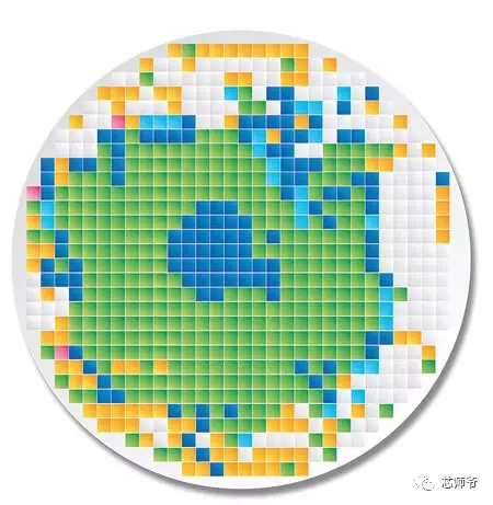
CP: Circuit Probe, wafer-level chip testing before packaging. This involves testing the chip's basic functions. Failures in different test items are shown in different colors. The failing items reflect chip design issues.
After passing these two stages, the wafer is diced. The diced chips are sorted according to the earlier results. Only good chips are sent to the packaging house. Packaging facilities are usually located near the fab because unpackaged chips cannot be shipped long distances. The package type depends on customer requirements—some need BGA, others need pins—but this step is simple and rarely fails. Since packaging yield is far higher than chip production yield, no testing is done after packaging.
FT: Final Test, performed after packaging. It is the closest to real-world use, covers more items than CP, and is where processors are sorted by frequency. Failures here reflect packaging-process issues, such as opens or shorts caused by poor wire bonding.
FT is the focus of the factory and requires extensive mechanical and automated equipment. Its purpose is to grade chips strictly. Taking Intel processors as an example, the following can occur during Final Test:
The chip passed WAT but is still bad.
Packaging damage.
Partial chip damage, e.g., two CPU cores are bad, the GPU is bad, or the display interface is bad.
The chip is good, with no faults.
Engineers must then work with marketing to decide how to grade these chips. For example, chips with a bad GPU can be sold as "Celeron" processors without a display core. Chips with two bad CPU cores can be sold as "Core i3" processors. Chips that work normally but at lower frequency can be sold as "Core i5" processors. Chips with no issues at all can be sold as "Core i7" processors.
How Is Final Test Performed?
Taking processors as an example, Final Test can be divided into two steps:
Automated Test Equipment (ATE)
System Level Test (SLT)
Step 2 is essential; step 1 is generally unaffordable for small companies.
ATE testing typically takes a few seconds, while SLT takes several hours; ATE greatly reduces chip test time.
ATE covers a great many items with strong logical dependencies. Tests must run in sequence, and later items may be skipped based on the results of earlier ones. The content of these items is proprietary, e.g., power supply checks, pin DC tests, logic tests (usually JTAG), burn-in, physical connection (PHY) tests, IP internal tests (including scan, BIST, function, etc.), IP IO tests (such as DDR, SATA, PLL, PCIe, Display, etc.), and auxiliary function tests (such as thermal characteristics, fuses, etc.).
Each test item yields a Pass/Fail result. Analyzing the chip's health from these results is the test engineer's job.
SLT is logically simpler: install the chip on a motherboard, configure memory and peripherals, boot an operating system, then run software stress tests, record and compare results. BIOS-related items are also checked.
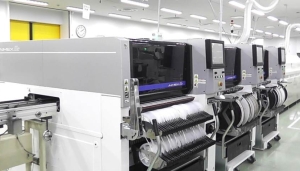
The image shows the layout of a test facility.
All of this must be designed by chip design engineers before tape-out. On-chip testing is handled by dedicated circuits built by DFT engineers. After tape-out, DFT engineers also generate the corresponding input vectors, typically tens of thousands of them. Whether these vectors can properly detect chip functionality must be ensured by product development engineers. In addition, test engineers, product engineers, and assistants work together to ensure that the daily production of tens of thousands of chips is not delayed by test-logic bugs.
Considering that each test-version iteration involves hundreds of thousands of lines of code, ensuring the code is error-free requires hundreds of test engineers working together—not counting production-line technicians—so testing is time-consuming and labor-intensive. In fact, for many large companies, chip testing costs are already approaching R&D costs.
WAT vs. FT
WAT identifies dies that fail testing; only dies that pass are packaged.
FT tests packaged chips and screens out nonconforming parts. Many WAT and FT items overlap; FT includes more functional tests.
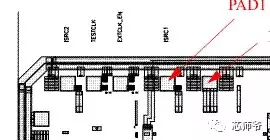
WAT requires probe contact with test pads. The main test items are:
Continuity Test (open/short)
Leakage Current Test (Stress Current Test)
Digital pin tests (input current/voltage, output current/voltage)
AC tests (scan test) and functional tests

TEL: 0731-85260926
Fax: 0731-85263946
E-mail: sales@jectronic.com
Address: Room 1015, Building A3, Changsha Yu Center, No. 289 Huanbao Middle Road, Yuhua District, Changsha City
Copyright © Changsha Ligao Jiechuang Instruments Co., Ltd.
Copyright Jectronic instruments ltd, All Rights Reserved
- IWATSU SY-8218 BH Analyzer Automated Operation Control Software SY-810
- T&M SSDN-414 CVR Double Pulse Ids Coaxial High-Frequency Precision Current Shunt for Double Pulse
- PD-200X Multi-Purpose Double Pulse (DPT) Device Dynamic Parameter Analysis System
- T&M A Series (4/5/6Watt) Precision Non-Inductive Coaxial Resistor
- IWATSU CS-8000 5KV/2KA New-Generation Semiconductor Parameter Analyzer
- IWATSU SY-8264 Series B-H Analyzer High-Frequency 30MHz Magnetic Loss System
- Cascade SUMMIT11000 200mm Manual Probe Station FormFactor 8-Inch
- Apollowave α-300 Apollo Microwave Manual 8-inch Probe Station

For more information, please follow our WeCom.

