 Technical Support
 Feedback



In-Depth Guide: V (BR) DSS Drain-Source Breakdown Voltage

1. Definition
V (BR) DSS: the drain-source avalanche breakdown voltage.
Standard test conditions: VGS = 0 V (gate shorted to source, device fully off). At a specified junction temperature, the drain-source DC voltage is slowly ramped up; the instantaneous voltage at which the drain current reaches the threshold current specified in the datasheet is V (BR) DSS.
This parameter defines the maximum voltage withstand limit of a SiC MOSFET and is the key red line for power device selection, overvoltage protection, and safe derating design.
The industry-standard voltage ratings of common 1200 V and 1700 V SiC devices are all specified against this parameter.
2. Underlying Device Physics
In the off state of a SiC MOSFET, the channel is fully turned off and no conductive inversion channel exists between source and drain.
The high-voltage region is the reverse-biased PN junction formed by the N+ drain → N− drift layer → P-body region.
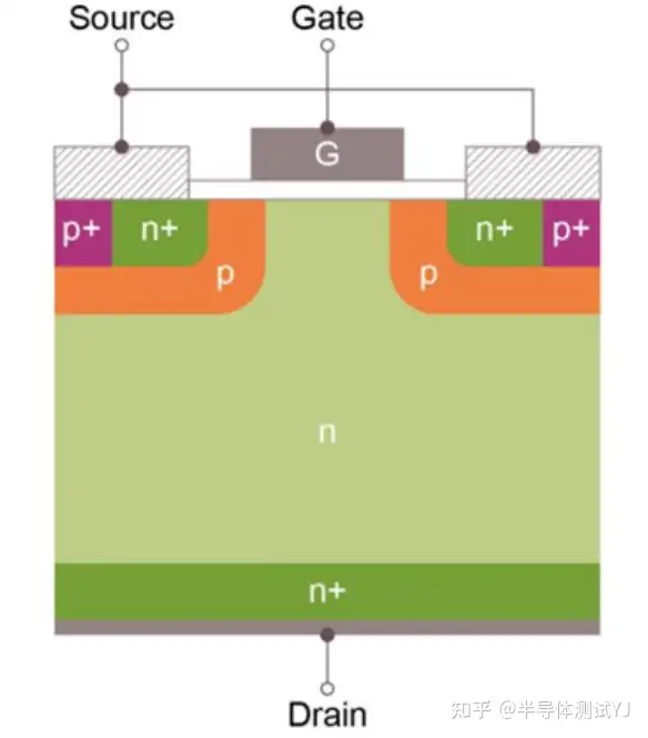
Normal off-state operation: the reverse PN junction is lightly reverse-biased, only a very small intrinsic leakage current flows, and the device insulates reliably.
As the voltage continues to rise: the depletion region widens continuously and the internal electric field strength increases linearly.
Reaching the critical field: once the intrinsic critical breakdown field strength of 4H-SiC is exceeded, avalanche breakdown is triggered; the strong electric field tears covalent bonds in the crystal lattice, instantly generating a large number of electron-hole pairs.
Failure signature: leakage current avalanches upward; without current limiting, this causes thermal destruction of the lattice and permanent, irreversible device damage.
Compared with silicon devices, SiC has a critical breakdown field roughly 10× that of silicon; for the same voltage rating, the drift layer is thinner and more heavily doped, naturally delivering the core advantage of "high voltage withstand + low conduction loss."
Key characteristic: V (BR) DSS has a positive temperature coefficient
A property unique to SiC: the higher the junction temperature, the higher the breakdown voltage.
Mechanism: high temperature intensifies thermal vibration of lattice atoms and enhances carrier scattering, so a higher reverse field is required to trigger avalanche.
Unlike silicon MOS/IGBT devices, which suffer from "falling voltage withstand at high temperature and easy thermal runaway," this is a core advantage of SiC power devices in high-temperature operation.
3. Application of 175°C High-Temperature Testing: Supporting Device Reliability Verification
SiC MOSFETs typically have a maximum rated junction temperature of 175°C. In high-frequency, high-power applications such as automotive, energy storage, and industrial power supplies, devices operate in elevated temperature ranges for extended periods.
In practice, V (BR) DSS can optionally be tested at 175°C, which also serves to verify the device's high-temperature reliability and provide reference data for device selection and long-term stable operation. Specifically, it enables the following:
Verify voltage-withstand stability at high temperature
By comparing V (BR) DSS data at 25°C and 175°C, you can directly assess voltage-withstand consistency at the extreme high-temperature limit, confirm that high temperature does not degrade the voltage-withstand characteristics, and ensure insulation reliability under long-term high-temperature operation.
Help screen out devices with process defects
High temperature amplifies latent process defects such as gate-oxide interfaces and PN-junction edge termination. If V (BR) DSS at 175°C shows abnormal variation or a low reading, a process defect can be preliminarily identified, enabling early screening of substandard parts and avoiding breakdown risk in later application.
Quantify high-temperature voltage margin to support design verification
V (BR) DSS data at 175°C, combined with room-temperature parameters, allows calculation of the breakdown-voltage temperature coefficient, providing data support for derating design and voltage-spike verification under high-temperature conditions, making circuit design more reliable.
Actual impact of 175°C on V (BR) DSS
Voltage value: for SiC MOSFETs of the same rating, V (BR) DSS at 175°C is 5%–15% higher than at 25°C, so the high-temperature voltage margin increases passively.
Leakage current baseline: at high temperature, intrinsic carrier generation surges and off-state leakage current rises significantly; datasheets correspondingly raise the breakdown detection current threshold at high temperature to avoid mistaking leakage for breakdown.
Structural stress: at high temperature, differences in the coefficients of thermal expansion of the package, solder, and die generate micro-stress, which slightly affects the voltage-withstand consistency of the edge termination.
4. Direct Impact on Circuit Design and Device Selection
Mandatory derating design guidelines

