 Technical Support
 Feedback



I. Standard Terminology Definition of IDSS

IDSS:Drain-source cutoff leakage currentFull English name: Drain-Source Leakage Current
Standard electrical definition:
When thegate and source are shorted, VGS=0V, the device is fully turned offUnder the premise that;
A rated high voltage VDS specified in the datasheet is applied between the drain and source;
At the specified reference temperature (room temperature 25°C, high temperature 150°C/175°C);
When the device is in the off steady state,The tiny reverse leakage current flowing from drain to source。
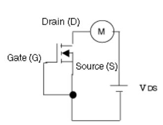
Plain explanation:
The SiC MOS is fully turned off with no turn-on voltage applied,
High voltage is applied between D and S, which should be nearly insulating,
But in reality there is stillWeak leakage, and this current is IDSS.
II. Underlying device physics of IDSS
1. Differences in drain leakage mechanisms between silicon MOS and SiC MOS
Silicon MOSFET off-state leakage current mainly comes from:
PN junction reverse saturation leakage + residual surface channel conduction.
The leakage mechanism of SiC MOSFETs is more special:
- SiC has a wider bandgap and lower intrinsic carrier concentration,Intrinsic baseline leakage is naturally smaller than that of silicon;
- There existsgate oxide interface defects, lattice vacancies, substrate microdefects, tunneling leakage is induced under high voltage;
- During high-voltage operation, the depletion layer in the drift region extends laterally, producingavalanche-induced leakage current;
- As temperature rises, a large number of intrinsic carriers are excited in the lattice,IDSS rises exponentially with temperature。
Core one-sentence mechanism
Even when the SiC MOS is fully turned off with zero gate voltage,
Subject tointerface defects, high-voltage depletion layer effects, and high-temperature intrinsic excitation,
a steady-state tiny leakage current still exists, which is IDSS.
III. Core differences in gate bias between SiC and silicon-based MOSFETs (key point)
When testing IDSS, the choice of gate bias method is a key difference between SiC and silicon-based MOSFETs, and also a common pitfall for engineers. The details are as follows:
1. Conventional testing practice for silicon-based MOSFETsWhen testing IDSS on traditional silicon-based MOSFETs, the industry generally adopts a "gate-source shorted, VGS=0V" bias method. Since silicon-based MOSFETs have a higher threshold voltage and relatively stable gate oxide interface characteristics, 0V gate voltage can reliably turn off the device, meeting the accuracy requirements of routine testing with good data repeatability.
2. Special characteristics of SiC MOSFETsUnlike silicon-based MOSFETs, SiC MOSFETs have two core characteristics that make testing IDSS with only VGS=0V limited:
(1) The threshold voltage VGS(th) of SiC MOSFETs is generally low, and the gate oxide interface is prone to state charges, which can easily induce residual surface channels;
(2) Under high-temperature conditions (such as 150℃, 175℃), the threshold voltage of SiC further drifts, and turn-off capability decreases.
If only VGS=0V bias is used, it is difficult to fully suppress the weak inversion channels remaining on the surface, which introduces additional false conduction current, causing the measured IDSS value to be too high. This cannot truly reflect the device's own high-voltage leakage level and may even lead to misjudgment of device quality.
3. Reasonable bias method for SiC MOSFET IDSS testingIn engineering testing and specification evaluation of SiC MOSFETs, some devices do not mandatorily require a negative gate voltage, but from the perspective of testing rigor, data consistency, and reliability assessment, applying the recommended turn-off negative voltage (such as -5V, -10V, -15V) for gate bias is more standardized and reasonable.
The core role of the negative gate voltage is to: fully deplete the residual surface channel, offset the influence of gate oxide interface charges, and ensure the device is in a truly fully off state. Especially under high-temperature and high-voltage test conditions, applying the recommended negative voltage makes IDSS test results closer to the device's true inherent leakage characteristics, reduces test errors, and provides more accurate data support for device reliability assessment.
IV. Practical impact of IDSS on complete circuit and reliability
- Increases static standby lossUnder equipment shutdown, standby, and no-load conditions, the leakage of multiple devices adds up, forming continuous static power consumption and raising the overall standby energy consumption of the equipment.
- Risk of thermal runawayIDSS has aPositive temperature coefficient: Temperature rises → leakage current increases → heat generation increases → temperature continues to climb Under sealed high-temperature conditions and multi-device parallel scenarios, a vicious cycle is easily formed, inducing thermal runaway.
- Reflects wafer and gate oxide qualityIDSS exceeding the limit directly corresponds to: wafer process defects, gate oxide interface degradation, and package insulation micro-leakage, which are important precursors to early device failure.
- Affects current-sharing consistency in multi-device parallel operationIf same-spec SiC MOS devices have large IDSS dispersion, inconsistent leakage under high-temperature off-state conditions will cause individual devices to bear heavier loads, accelerating aging degradation.
- Core: criterion for mass production screeningIf IDSS exceeds the datasheet threshold, it is directly judged as electrically defective and cannot be used on board; this is a hard failure parameter.
V. Three conditions to watch closely when reading IDSS in datasheets
When reading the IDSS value in a SiC MOSFET datasheet, do not look only at the current magnitude; you must also pay attention to its test limiting conditions, otherwise the data has no reference value. The three core conditions are as follows:
1. Gate bias condition: Silicon-based MOSFETs mostly specify VGS=0V; for SiC MOSFETs, attention must be paid to the recommended turn-off negative bias condition (such as -5V) in the datasheet, and testing must strictly match this condition to ensure data consistency.
2. Drain-source voltage VDS: IDSS testing requires applying the VDS corresponding to the device's rated voltage class (such as 650V, 1200V, 1700V). IDSS values vary greatly under different VDS, and test data not matching the rated VDS is invalid.
3. Temperature condition: Datasheets usually provide both the 25°C room-temperature and 150°C/175°C high-temperature IDSS typical values. Looking only at room-temperature data cannot evaluate the leakage degradation characteristics of the device under actual high-temperature conditions, so high-temperature data must be considered for comprehensive judgment. In fact, this is also reasonable. In actual testing, a customer with AI server power supplies reported that a certain domestic SiC MOSFET had very severe leakage at high temperature, making device reliability questionable.
VI. Professional details to note when testing IDSS
- Must wait for complete thermal equilibriumIDSS is extremely sensitive to temperature, and slight temperature drift will cause current reading deviation. Wait for the value to fully stabilize before collecting data; do not use fixed-time rough measurement.
- Avoid airflow and ambient temperature field disturbanceAir convection and airflow fluctuations cause slight fluctuations in device surface temperature, directly causing nA/μA-level leakage current drift. Weak leakage testing must maintain a static temperature field free of convection interference, preferably with windless heating.
- The wafer must be shieldedIDSS and V(BR)DSS actually differ very little under the test environment. In many cases, customers report that during wafer-level testing, the breakdown voltage is lower than in previous tests and IDSS increases. This is often because the probe station shielding enclosure was not properly closed or the internal light source of the probe station was not turned off. An unclosed light source generates photo-generated carriers that interfere with the device's leakage and breakdown characteristics; if the shielding enclosure is not tightly closed, external electromagnetic interference and stray signals are introduced, causing test data distortion. Therefore, during wafer-level testing, it is essential to ensure that the probe station shielding enclosure is closed and the internal light source is off, ensuring a sealed and interference-free test environment. Summary
- Never leave the gate floatingThe test fixture must ensure that the G terminal is reliably shorted to the S terminal. Once the gate is left floating and induces a weak voltage, it will directly change the conduction state, and the IDSS test result will be completely distorted. In particular, SiC devices have a relatively low threshold voltage, and interface states are likely to exist at the gate oxide interface, which can easily induce residual surface channels, making them prone to false turn-on; moreover, the threshold voltage is more likely to drift at high temperatures, so this situation must be avoided. It is recommended to use a turn-off negative voltage to set the gate bias. Compared with zero-bias testing, this can effectively reduce the impact of false conduction current, making the data more rigorous and repeatable. In actual testing, it is preferred to set the S terminal to 0V/GND, and for the G terminal, preferentially use a negative voltage (preferably as recommended in the datasheet) and 0V. Connecting the S terminal and G terminal to 0V is better than connecting them to GND, because 0V is a stable potential reference, which can effectively avoid interference caused by the small potential difference between "instrument ground" and "measurement ground," further ensuring test accuracy. Be sure to avoid leaving any terminal floating.
- Test and compare high and low temperatures separatelyTesting only at room temperature cannot reflect true reliability. It is necessary to test separately at room temperature and rated high temperature, observe the degree of leakage degradation with temperature, and evaluate the device quality margin.
VII. Summary
IDSS is the inherent leakage current of SiC MOSFETs under high-voltage off-state conditions. Its magnitude is jointly determined by gate oxide interface characteristics, high-voltage depletion layer effects, and high-temperature intrinsic excitation, and it is a core parameter for measuring the off-state insulation performance and reliability of the device.
Unlike traditional silicon-based MOSFETs, SiC MOSFETs tested for IDSS using only zero gate voltage often cannot fully suppress residual surface channels, resulting in data distortion; applying the recommended turn-off negative bias per the datasheet is a more standardized and reasonable engineering test method, making leakage data more realistic and more valuable for reference.
In practical applications and testing, it is necessary to focus on the test limiting conditions of IDSS, standardize the test process, and comprehensively evaluate by combining room-temperature and high-temperature data, so as to accurately judge the true performance and quality of SiC devices and avoid circuit faults and reliability risks caused by abnormal leakage.
This series will continue. Everyone is welcome to exchange friendly comments in the comment section, and please look forward to the next installment!

